Controlling the Si5351

The venerable Si5351 pops up in a lot of applications related to amateur radio as a convenient and flexible Direct Digital Synthesizer (DDS). It is a device primarily designed to replace crystals, oscillator circuits and PLLs used in digital systems to provide clocks used by, for example, ethernet, HDMI and USB controllers.
In this article, I’ve collected some notes on understanding the logic and workings of the device and how to configure it to produce a desired frequency output. Of course, there exist many good libraries for controlling it from a number of platforms, but it’s nice to have a lower level understanding of what’s happening inside, and there are some interesting concepts such as phased locked loops and continued fractions that are worth knowing about.
Throughout this, I’m going to refer exclusively to the (probably more common) Si5351A (revision B) model, i.e. the one with the requirement for a reasonably stable external crystal reference frequency.
Selecting an approach for determining the parameters to load in to the Si5351 will be a trade-off for your particular circumstances, balancing the frequency range, number of outputs in use, and necessary accuracy. The approach described here is possibly the most basic but should also lead to the most accurate synthesized frequency achievable, at the expense of not being able to generalise across a wide frequency range.
The code shown here is in python for calculating offline (chosen simply because it’s clearer when writing) - but could almost be copied-and-pasted directly into C/++ code.
Si5351 Overview
The Si5351 produces a square wave (unlike the AD9834 which produces a sine wave) output by multiplying up a reference frequency using a Phase Locked Loop (PLL), then dividing this frequency to form the output frequency. A very simplified overview of these stages is shown in the diagram below.
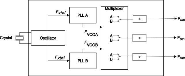
Here we see that the reference crystal drives an oscillator, which in turn forms the input to two Phase Locked Loops (PLL). Each output has its own frequency divider, and the input to each divider can be switched between either one of the PLLs.
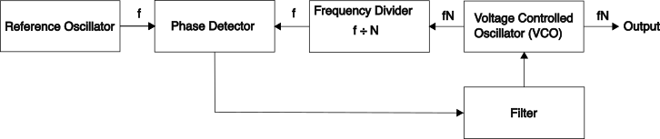
Phase Locked Loop (PLL) Recap
It’s good to understand what’s going on inside a PLL. At its simplest, a PLL is a circuit or system that will aim to match produce an output signal with a constant phase difference to an input reference signal:
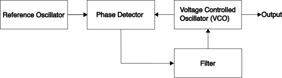
Without describing how these blocks would be implemented, the key components are the phase detector and loop filter - that form a feedback system to the Voltage Controlled Oscillator (VCO). The phase detector detects the phase difference between the two signals, and this is smoothed by the loop filter. The resulting signal is then fed to the VCO to control the output frequency - with the goal of ensuring that a constant phase difference in the signals.
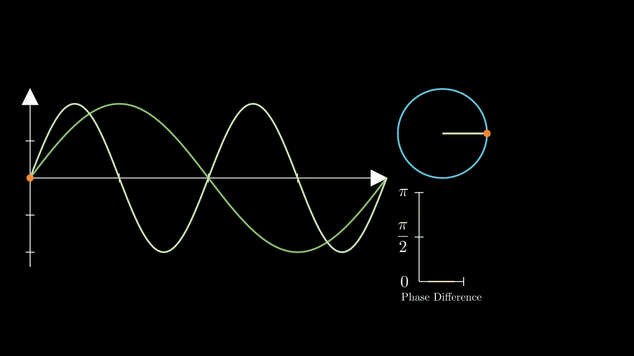
Recall that if we have two different frequencies their phase differences will be constantly changing - as illustrated here:
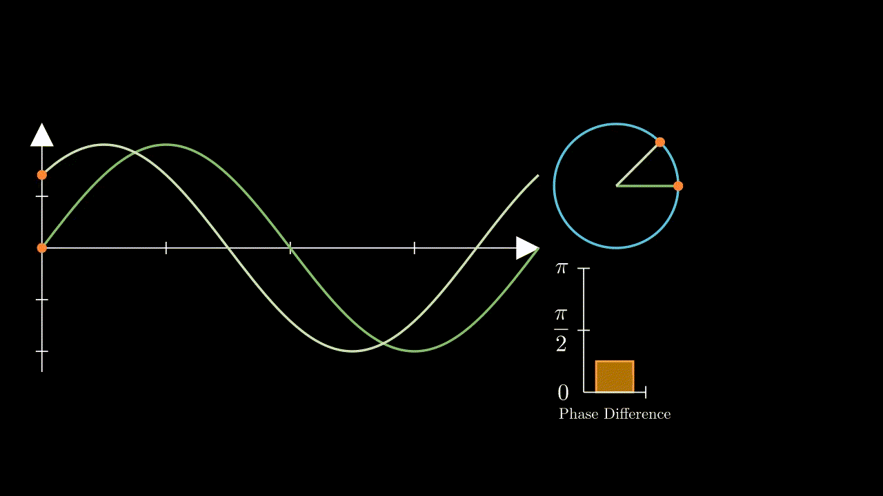
Whereas two equal frequencies, even having a phase offset to one another, will have a constant phase difference:
Therefore - at its most basic level, all a PLL will do is create a frequency output that matches its reference input. This doesn’t sound particularly useful, however with a simple change, it can become very relevant to our needs here in order to create a digitally controlled oscillator. By adding a frequency divider block between the VCO and phase detector, that divides its input frequency from the VCO by some value \(N\), we would effectively create a frequency multiplier - as the system forces the VCO to oscillate at \(N\) times the input frequency in order to achieve a constant phase difference with the frequency coming from the divider:
Back to the Si5351… We learn from the application note that the PLLs can generate an output frequency of between 600 - 900MHz, and that supported crystal values are either 25 or 27MHz.
The key information for setting our frequency of choice is the equation for both the PLL multiplier and final frequency divider:
\[F_{vco} = F_{xtal} \times (a_{p} + {b_{p} \over c_{p}}) \]
where \(F_{vco}\) and \(F_{xtal}\) correspond to the frequencies shown in the block diagram of the Si5351, and \(fN\) and \(f\) respectively in the PLL diagram above. For the final stage - the equation is similar, for frequencies below or equal to 150MHz, where \(a >= 8\) (for frequencies above 150MHz, the value of the divider must be one of 4, 6, or 8 - and the PLL adjusted accordingly):
\[F_{out} = {F_{vco}\over{a_{m} + {b_{m}\over{c_{m}}}}}\]NB: \(a_{p}\) and \(a_{m}\) (along with \(b\) & \(c\)) denote the values of \(a\) (and \(b\) & \(c\)) for the pll and multisynth (the manufacturer’s name for the divider circuit) respectively.
(There is also an additional ‘R’ integer divider after this Multisynth divider, which we’re going to ignore to focus on the fractional part here)
As the PLL is, unlike the final divider, a feedback system, it is recommended that in order to avoid frequency jitter, the value of the final divider is set as an integer value.
Calculating PLL & Divider Coefficients - Continued Fractions
The PLL equation has a valid range \(a + {b \over c}\) of between \( 15 + {0 \over 1048575} \) and \( 90 \) I.e., the minimum value for \( a \) is \(15\), maximum values for \(b\) and \(c\) are 1,048,575 and no combination of coefficients can give a result greater than 90.
To determine values for these parameters for our desired multiplier (in the case of the PLL) or divider, we can treat this equation as a continued fraction - that is more generally, an expression that can be written as:
\[ x = b_{0} + {a_{1}\over{ b_{1} + {a_{2}\over{b_{2} + {a_{3}\over{b_{3} + {a_{4}\over{b_{4}...}}}}} }} } \]It has been proven, that for all rational values, it is possible to represent this value as a simple continued fraction, in which case - all values for \(a\) can be set to 1, and furthermore, the fraction will eventually terminate with some finite number of terms (which could be quite large admittedly). To determine these terms for a target value, an algorithm called Euclid’s Algorithm could be used.
Euclid’s Algorithm
Because the values that we want to use to control our Si5351 are quite large, let’s illustrate the algorithm with something smaller. Say we wish to express \(159 \over 15\) in our \(a + {b \over c}\) format. (We could think of this as what value would we need to set for a PLL multiplier to multiply a 15Mhz reference signal by to obtain a 159MHz output signal?)
Euclid’s algorithm tells us to do the following:
Let the two positive integers in our fraction be denoted by \(u\) and \(v\)
Inialise an empty list/vector of integers to hold our values for \(b\)
- If \(u < v \), swap them
- Divide \(u\) by \(v\), append the integer (floored) result to the back of our list, and find the remainder \(r\)
- If \(r = 0 \), terminate
- Otherwise, set \( u = v \) and \(v = r\) and repeat from step 1
Python code
u = 159
v = 15
b = []

MAX_ITERATIONS = 100

while len(b) < MAX_ITERATIONS:
    if u < v:
        u, v = v, u
    b.append(int(u / v))
    r = u % v
    if r == 0:
        break
    u = v
    v = r
Running this algorithm for our example of \(u = 159\), \(v = 15\) results in an output of \(b = [10,1,1,2] \) which corresponds to:
\[
{159 \over 15} = 10 + {1\over{ 1 + {1\over{1 + {1\over{2}}}}}}
\]The first 10 there should be pretty obvious, but how do we make sense of the rest of it? We’ll need to also describe an algorithm for converting our list of coefficients to a set of 3 values for \(a + {b \over c}\), but first let’s verify that the solution is actually correct. Let’s work it out manually right-to-left from our list of values for \(b\) - or bottom to top in our continued fraction:
\[
10 + {1\over{ 1 + {1\over{1 + {1\over{2}}}}}} = 10 + {1\over{ 1 + {1\over{3\over{2}}}}} = 10 + {1\over{ 1 + {2\over{3}}}} = 10 + {1\over{{5\over{3}}}} = 10 + {3\over{5}}
\]Technically we could go one step further too and represent this as \(10 + {3 \over 5} = {53 \over 5}\). This is helpful for the next step, which is to define the algorithm for converting our list of values for \(b\) into a single fraction.
Suppose that this final value (in this example \( { 53 \over 5}\) ) could be represented by a fraction \({P_{k} \over Q_{k}}\), and we are given some finite list of values \([b_{0}; b_{1}; b_{2} ... b_{k}] \) - where \(b_{n}\) are all positive integers, to represent our simple continued fraction, we can use the following algorithm to represent them as a single fraction, that, importantly, cannot be reduced any further.
-
Define \( P_{-1} = 1,\text{ }P_{0} = b_{0},\text{ }P_{k} = b_{k}P_{k-1} + P_{k-2} \)
and \(Q_{-1} = 0,\text{ }Q_{0} = 1,\text{ }Q_{k} = b_{k}Q_{k-1} + Q_{k-2} \)
-
Recursively solve for the above values of \(P_{0...k}\) and \(Q_{0...k}\) for values of \(b_{0...k}\), the final value of \(P_{k} \over Q_{k}\) being our result, E.g.:
| k |
-1 |
0 |
1 |
2 |
3 |
| b |
n/a |
10 |
1 |
1 |
2 |
| P |
1 |
10 |
\(1 \times 10 + 1 = 11\) |
\(1 \times 11 + 10 = 21\) |
\(2 \times 21 + 11 = 53\) |
| Q |
0 |
1 |
\(1 \times 1 + 0 = 1 \) |
\(1 \times 1 + 1 = 2\) |
\(2 \times 2 + 1 = 5\) |
Python code
def parameter(param_k_minus_two: int, param_k_minus_one: int, b: list[int]) -> int:
    value = b[0] * param_k_minus_one + param_k_minus_two
    if len(b) == 1:
        return value
    return parameter(param_k_minus_one, value, b[1:])


P = parameter(1, 10, [1, 1, 2])  # = 53
Q = parameter(0, 1, [1, 1, 2])  # = 5
Transforming improper fraction back to our desired \(a + {b\over{c}} \) format is simply a case of assigning \(a = b_{0} \) and \(b = P_{k} \bmod Q_{k}\).
Calculating Si5351 Values - Basic Algorithm
Now let’s put this all together. Say we wish to use our DDS to generate frequencies on the HF amateur bands. As an example, we might want to generate a stable frequency at 14095.6 KHz. A simple algorithm to determine the parameters needed might follow as:
Given:
CRYSTAL_MHZ as the value of the crystal in MHz (in this case 27)PLL_MIN as the minimum acceptable value for the PLL in Hz (in this case, 600e6)- A target value
target_freq_hz as the desired output value in Hz
Then:
- Assign the variable
divider = CRYSTAL_MHZ
- Assign the variable
pll_out = target_freq_hz * divider
- Assign the variable
c = 0
- While
pll_out < PLL_MIN_HZ, increment divider by one and repeat step 2.
- If
c != 0 increment divider by one and recalculate the value for pll_out as in step 2
- Use the previous algorithms for determining quotients and parameters in order to describe the value for PLL out.
- While
c > 1048575, repeat from step 5.
Python code
MAX_ITERATIONS = 100


def quotients(_a: int, _b: int) -> list[int]:
    a, b = _a, _b
    out: list[int] = []
    while len(out) < MAX_ITERATIONS:
        if a < b:
            a, b = b, a
        out.append(int(a / b))
        r = a % b
        if r == 0:
            break
        a = b
        b = r
    return out


def parameter(
    param_k_minus_two: int,
    param_k_minus_one: int,
    b: list[int],
    max_value: None | int = None,
) -> int:
    value = b[0] * param_k_minus_one + param_k_minus_two
    if len(b) == 1:
        return value
    return parameter(param_k_minus_one, value, b[1:])


CRYSTAL_MHZ: int = 27
PLL_MIN_HZ: int = 600e6
target_freq_hz: int = 14095600
divider = CRYSTAL_MHZ

pll_out = target_freq_hz * divider
while pll_out < PLL_MIN_HZ:
    divider += 1
    pll_out = target_freq_hz * divider


a = b = c = 0

while c > 1048575 or c == 0:
    if c > 0:
        divider += 1
        pll_out = target_freq_hz * divider

    Q = quotients(pll_out, CRYSTAL_MHZ * 1e6)
    O = parameter(1, Q[0], Q[1:])
    P = parameter(0, 1, Q[1:])

    a = Q[0]
    b = O % P
    c = P

print(f"{a=}, {b=}, {c=}, ({divider=}, {pll_out=})")
In this example, we end up with the the values for the PLL as \(a_p = 22\), \( b_p = 30277 \), and \( c_p = 67500 \) to give us a PLL value of 60611080Hz and a divider of 43 (which we could represent as \(a_m = 42\), \(b_m = 1\), \(c_m = 1\)). We can also validate that dividing the PLL value by the divider gives us exactly the input frequency we desire.
Of course, there are some assumptions here that we’ll never go above the maximum allowable PLL value, and also it should be clear that there will end up being cases where this algorithm would only result in an approximation for the frequency value - particularly as we might wish to generate frequencies with finer precision (or even non-integer frequencies). To handle these cases, we would probably need to relent and use a non-inter value for a final divider. However, for the moment, let’s continue with this and complete the steps needed to get the chip to actually produce a signal.
Si5351 Register Setup
Now let’s set the chip up and push these values in. In the application note, we learn that the values we have calculated are represented in register space across three 18 - 20 bit values, P1 - P3, as:
\[
P1[17:0] = 128 \times a + \lfloor{128 \times {{b}\over{c}}}\rfloor - 512
\]
\[
P2[19:0] = 128 \times b - c \times \lfloor{128 \times {{b}\over{c}}}\rfloor
\]
\[
P3[19:0] = c
\]
These values are each split across multiple 8 byte registers, although not all bits are used for this in all registers, and it’s important to be careful with the precise ordering. For the above example frequency, here are the values for the bytes shown in the register map for PLLA and MS1, along with python code for producing these:
(PLL A \(F_{\text{out}} = 606110800\text{Hz}\), \(F_{\text{xtal}} = 27\text{MHz} \)):
\[a_{p} = 22 \quad b_{p} = 30277 \quad c_{p} = 67500\]\[P1_{p} = 2361 \quad P2_p = 27956 \quad P3_p = 67500 \]
| Register |
Description |
Value |
| 26 |
MSNA_P3 [15:8] |
0x07 |
| 27 |
MSNA_P3 [7:0] |
0xac |
| 28 |
7-2 Reserved MSNA_P1 [17:16] |
0x00 |
| 29 |
MSNA_P1 [15:8] |
0x09 |
| 30 |
MSNA_P1 [7:0] |
0x39 |
| 31 |
MSNA_P3 [19:16] MSNA_P2 [19:16] |
0x10 |
| 32 |
MSNA_P2 [15:8] |
0x6d |
| 33 |
MSNA_P2 [7:0] |
0x34 |
And for our divider (MS1), which we shall set to the integer value of 43:
\[a_{m} = 42 \quad b_{m} = 1 \quad c_{m} = 1\]
\[P1_m = 4992 \quad P2_m = 0 \quad P3_m = 1 \]The general layout of the register for the multisynths matches that of the PLL, apart from the 3rd byte where some of the 6 reserved bits are used to select further config (described below):
| Register |
Value |
| 50 |
0x00 |
| 51 |
0x01 |
| 52 |
0x00 |
| 53 |
0x13 |
| 54 |
0x80 |
| 55 |
0x00 |
| 56 |
0x00 |
| 57 |
0x00 |
The python code to compute these values is here:
Python code
def set_register(a: int, b: int, c: int) -> list[int]:
    P1 = 128 * a + floor(128 * b / c) - 512
    P2 = 128 * b - c * floor(128 * b / c)
    P3 = c

    print(f"{P1=}, {P2=}, {P3=}")

    regs: int = [0] * 8
    regs[0] = (P3 >> 8) & 0xFF
    regs[1] = P3 & 0xFF
    regs[2] = (P1 >> 16) & 0x03
    regs[3] = (P1 >> 8) & 0xFF
    regs[4] = P1 & 0xFF
    regs[5] = ((P3 >> 12) & 0xF0) + ((P2 >> 16) & 0x0F)
    regs[6] = (P2 >> 8) & 0xFF
    regs[7] = P2 & 0xFF

    return regs

pll_regs = set_register(22, 30277, 67500)

PLL_A_REG_START: int = 26
for idx, value in enumerate(pll_regs):
    print(f"{PLL_A_REG_START + idx}: {hex(value)}")

ms_regs = set_register(42, 1, 1)

MS_1_REG_START: int = 50
for idx, value in enumerate(ms_regs):
    print(f"{MS_1_REG_START + idx}: {hex(value)}")
Device Setup
There are a few more options that we need to configure to set up our device for producing a frequency:
- The Crystal Load Capacitance Selection (register 183)
- Clock input source select (bits 3:2 of register 16 + N where N is the clock number in CLK N)
- Multisynth source select for Clock (bit 5 of register 16 + N)
- Multisynth integer mode (bit 6 of register 16 + N)
- Clock drive strength control (bits 1:0 of register 16 + N )
- Output (R) divider values, & divide by 4 enable (bits 6:4 and 3:2 of the 3rd byte of the appropriate multisynth register)
- Output enable control (register 3)
Check the application note for values that would match your configuration. For the most part, the defaults are sensible although getting the correct crystal load capacitance and drive strengths are important.
Finally, when writing the initial values to the device, the datasheet recommends following a particular order with disabling the outputs, powering down the output drivers, configuring the outputs and drivers, and then resetting the PLLs followed by enabling the outputs.
Let’s now bring it all together and get a signal out. In this setup I’ve used the RP2040 and its C++ API to communicate with the device over I2C, with the values calculated with the above code:
C++ Code for RP2040/50
#include <hardware/gpio.h>
#include <hardware/i2c.h>
#include <pico/stdio.h>
#include <pico/time.h>
#include <stdlib.h>
#include <string.h> // memcpy

#include <cstdint>
#include <stdint.h>
#include <stdio.h>


constexpr uint8_t I2C0_SDA = 24;
constexpr uint8_t I2C0_SCL = 25;

constexpr uint8_t SI5351_BUS_ADDR = 0x60;

constexpr uint8_t SYS_INIT_BIT = 7;


uint8_t read_byte(uint8_t addr){
	uint8_t buffer = addr;
	i2c_write_blocking(i2c0, SI5351_BUS_ADDR, &buffer, 1, true);
 	i2c_read_blocking(i2c0, SI5351_BUS_ADDR, &buffer, 1, false);
 	return buffer;
}

int write_bytes(uint8_t addr, uint8_t length, uint8_t *data){
	uint8_t tx_buffer[257];
	tx_buffer[0] = addr;
	memcpy(&tx_buffer[1], data, length);
	return i2c_write_blocking(i2c0, SI5351_BUS_ADDR, tx_buffer, (length + 1), false);
}

int write_byte(uint8_t addr, uint8_t value){
	auto val = value;
	return write_bytes(addr, 1, &val);
}

int main(){

	// Used to enable programming / reboot
	// without disconnecting
	stdio_init_all();

	i2c_init(i2c0, 400000);
	gpio_set_function(I2C0_SDA, GPIO_FUNC_I2C);
	gpio_set_function(I2C0_SCL, GPIO_FUNC_I2C);
	gpio_pull_up(I2C0_SDA);
	gpio_pull_up(I2C0_SCL);

	// Before writing anything to the device, wait
	// for it to be ready
	// uint8_t system_status = 0xFF;

	uint8_t system_status = read_byte(0);
	while(system_status >> 7){
		system_status = read_byte(0);
	}

	// Disable all outputs
	write_byte(3, 0xFF);

	// Power down all (8) output drivers
	uint8_t output_powerdown[8] = {0x80,0x80,0x80,0x80,0x80,0x80,0x80,0x80};
	write_bytes(16, 8, output_powerdown);

	// Set the crystal load capacitance (10pF)
	write_byte(183, 0xD2);

	// Now set up our PLL and MS params

	// PLLA - (27MHz Crystal) 606.1108MHz
	uint8_t PLLA[8] = {0x7, 0xac, 0x0, 0x9, 0x39, 0x10, 0x6d, 0x34};
	write_bytes(26, 8, PLLA);

	// MSN1 - Divide by 43
	uint8_t MSN1[8] = {0x0,0x1,0x0,0x13,0x80,0x0,0x0,0x0};
	write_bytes(50, 8, MSN1);

	// Power up the output driver for output 1, set 8mA drive
	// current, and integer mode
	write_byte(17, 0x4F);

	// Reset both PLLs
	write_byte(177, 0x20);
    write_byte(177, 0x80);

    // Enable output 1
    write_byte(3,0xFD);

	while(1){
	}
	return 0;
}
And finally - an output! Shown here is the trace across a 50 ohm resistor.
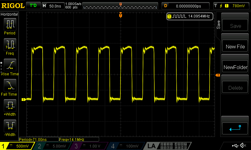
Error Correction
We see above that there is some slight error of 200Hz in the output. An interesting feature of the chip is the ability to drive an output directly with the crystal oscillator. In the case of output 1, we set bits 3 and 2 of register 17 to 0, and we also need to enable the fanout of the crystal oscillator by setting bit 6 (XO_FANOUT_EN) of register 187 to 1.
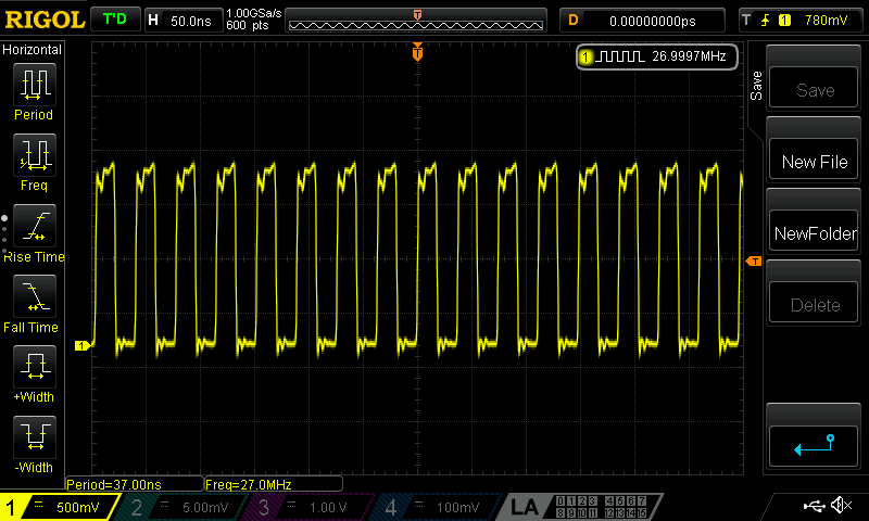
We can see now that the frequency of the crystal oscillator is 26.9997MHz (the counter on this scope has the a precision of 100Hz). If we then assume a 300Hz error we can check the PPM error of the crystal simply as \(300 \div 27 = 11.1\) which is slightly higher than the quoted accuracy of this crystal (+/-10ppm). Interestingly though, our final output frequency suggests an error of \(200 \div 14.0956 = 14.18\) ppm. Simply adding 200Hz to the desired output and re-running the calculations to determine the parameters for the PLL and divider does however give a stable output at the desired 14.0956MHz.
Conclusion
This method is one of many that can be used to select parameters to control the output frequencies of the Si5351. The ultimate strategy to choose would be a tradeoff between the flexibility needed at runtime, the accuracy and stability needed for the output signal, and also the number of outputs in use (i.e, more than two would mean needing to share a PLL). Whilst it may seem daunting at first though, through clever use of both PLL and Multisynth dividers, it should be possible to output effectively any frequency within the limits of the device, with very little external support circuitry.
References